eCADSTAR Advanced HS
Starting from £271 per month










eCADSTAR Advanced 3D Pricing
For more information please contact us today!
- Phone
Already have a licence and looking for a renewal quote? Click here
What Can You Do With ADVANCED 3D Compared to BASE?
eCADSTAR ADVANCED 3D includes three extra capabilities:
3D Collision Check identifies collisions between your PCB and external mechanical objects such as enclosures
3D Model Manager makes it easier to import and organize 3D models for parts in your library
STEP I/O provides import and export of mechanical data in this popular 3D model format, in addition to 3D model import and management
Creepage & Clearance Check checks for risky current leakage paths in three dimensions, even if current passes through objects like slots or un-plated holes. All this is in addition to clearance rules. eCADSTAR Advanced 3D is for engineers who design PCBs in context with mechanical objects and verify electrical safety in three dimensions.
The optional features that can be included in the ADVANCED 3D bundle are:
Autorouter
Gerber Import

2D/3D Design Optimisation
eCADSTAR offers design variation management tools that are suited for a wide variety of industries, control your products your way.
Use our advanced 3D collision and creepage check technology to catch enclosure issues and verify electrical safety early in the design process.

Smooth Integration
Export STEP models in 3D to work smoothly with mechanical CAD.
Import 3D models in multiple formats to organise your PCB relative to external 3D objects.
Export and import Gerber data which transforms photo data into real, editable eCADSTAR PCB Data. eCADSTAR’s intelligent, adaptive import means you can re-use and repurpose your artwork data without limits.
Included Features for eCADSTAR Advanced 3D
Get Results With Schematic Editor— Consistent, Connected, Comprehensive
Schematic Editor is eCADSTAR’s design capture application—a key part of our unified, internet-connected EDA solution for PCB design. eCADSTAR applications are clear and consistent. You work quickly and correctly. One user interface style. Universal web connectivity. Industry-proven technology. A short learning curve, but all the detailed features you need to optimize your designs.
Instant Web Part Access
Save time when you prototype, even before the new components you’re using are in your master library. Download what you need and carry on working. Find a web part, place it and it becomes part of your schematic. Forward-annotate to PCB Editor. No need for a final form factor yet. Create a prototype in seconds—check it out in 2D and 3D physical context right away.
Web part lookup is part of eCADSTAR’s connected design platform, with access to extensive online parts libraries, including 3D models—and downloaded parts are fully editable.
Block Hierarchy
Schematic blocks make your design easier to understand. They are great for design reviews and they equip you for maximum re-use, design integrity and teamwork. It’s easy to share blocks with other engineers, so you can refine, optimize, and keep similar circuits consistent.
Schematic blocks are parts of a schematic design that you identify and save as re-usable work during schematic capture. This means you can share them with other engineers. Blocks add hierarchy. A hierarchical PCB design adds structure, making electronic designs easier to interpret in reviews. It empowers concurrent design and simultaneous working on parts of a PCB design or system.
Design Variation
Structure design variation from schematic entry through to physical design. Decide which components are fitted and even which parts are used in each variant. A way to think of variation is that the conductor metal on the PCB is always the same, but you can vary what is assembled on it.
Design variation is how you manage different varieties of the same bare-board PCB without duplicating the parts that do not change. For example, premium versions of a PCB could include additional HDMI or USB ports or more memory.
Signal Integrity
Good signal integrity is essential for many PCBs, even if the products they go into are not high-speed. Many standard parts, including memory and I/O, run at high speeds. This means they use up less PCB real estate, because signals that run faster can travel over fewer tracks. eCADSTAR supports professional signal integrity control in both schematic entry and physical PCB design, using consistent methods throughout. In Schematic Editor, you can use simulation and analysis to see how your proposed layer stacks, track widths, spacings, etc. will perform when they are laid out on a PCB. Even better, when you’ve decided what you want, you can instantly create a PCB prototype and lay out as much or as little as you like. Then you can drill down to fine detail, using the same simulation and analysis you used in Schematic Editor.
Control high-speed layout without external software in a consistent, unified environment. Check the high-speed performance of proposed topologies, layer stacks, track widths, track spacings and PCB materials before you commit to physical design. PCB signal integrity tools used to be bolt-on, with a variety user interfaces. With eCADSTAR, what you need to achieve good signal integrity is built-in.
Collaboration
eCADSTAR is a next-generation solution, not a collection of disparate EDA applications strung together to address new issues as they emerged. Want to copy a circuit or a block from one schematic to another? Just open both then select, copy, paste. Want to share a high-speed scenario and its simulation results with another engineer? Just save and send. That engineer can open them and even edit them, sharing their suggestions back to you in the same way.
Multi-Instanced Hierarchy
Structure your schematics to maximise re-use opportunities and minimise copy/paste errors with multi-instanced hierarchy. It provides block structure with clear functional overviews and declutters reviews of circuits containing multiple channels (like Audio circuits).
Furthermore, define one block and create as many instances as you need in addition to avoiding copy/paste in channeled or repeated sections of circuitry, such as multiple USB I/O circuits. Plus upgrade key schematic circuits quickly and safely by instantly propagating block enhancements to their instances.
SPICE Controller
SPICE Controller is best paired with LTspice®, which is free to download and use. Simulate analog circuits while keeping key simulation setup with your schematic design. That makes analog circuits much easier to manage, review and re-use, even for single-board multi-technology PCBs.
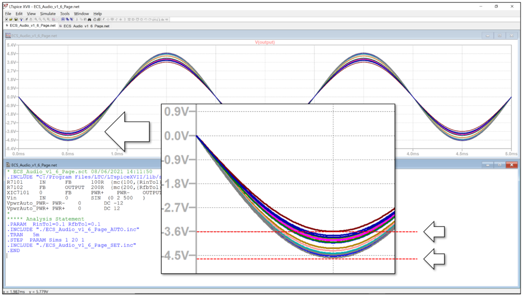
Successful analog simulation requires precise setup. Benefit from the industry-proven analogue simulation facilities of LTspice® with simulation data that is much easier to set up and manage.
Local Parts, Web Parts, PCB Technology and Design Rules
Library Editor is eCADSTAR’s library management application—a key part of our unified, internet-connected EDA solution for PCB design. Fast, consistent, and connected. Easy to learn, but with the power you need to create and maintain consistent core library data.
Library Editor provides everything you need for library management in one place. Naturally, it complies with the same user interface style as other eCADSTAR core applications. All this means there’s a single short learning curve that gets engineers up to speed super-fast.
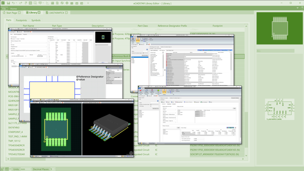
Library Editor combines all library editing and management in a single application—parts, schematic symbols, PCB footprints, pads, 3D models, web parts download and merge, PCB technologies, and design rules.
PCB Technology & Design Rules
PCB technology and design rules are part of your master library. You manage them in Library Editor, just as you do with other library data, so there is just one short learning curve.
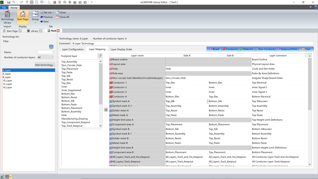
PCB technology and design rules are structured for maximum re-use. That does more than save valuable time—re-entered data is error-prone data.
With eCADSTAR, once data is entered and verified, it becomes premium IP that you can build on with confidence.
A layer stack need not be identical to re-use a PCB technology. If the top and bottom PCB layers, or a pair of inner layers are the same, then it’s much safer and more efficient to reference just one master definition. If a set of spacing or track width rules are the same on completely different layers, then the same applies—define once and then reference as many times as you like.
A layer stack need not be identical to re-use a PCB technology. If the top and bottom PCB layers, or a pair of inner layers are the same, then it’s much safer and more efficient to reference just one master definition. If a set of spacing or track width rules are the same on completely different layers, then the same applies—define once and then reference as many times as you like.
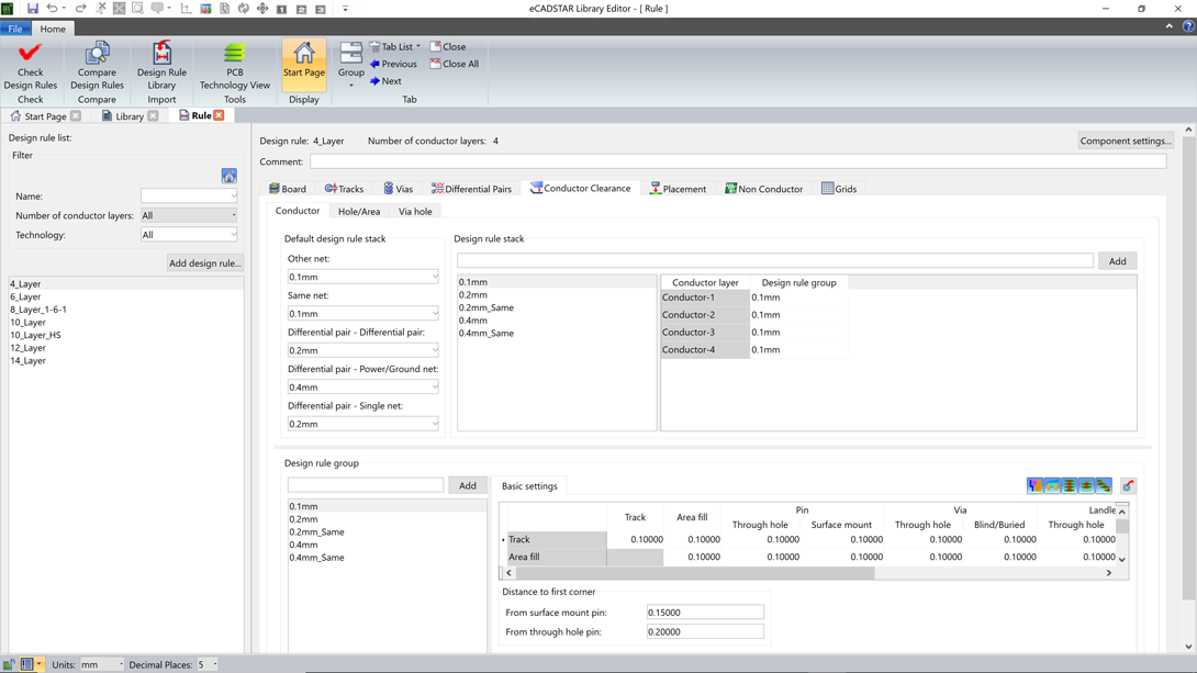
This philosophy carries over into the PCB design itself. If your PCB layout has a different number of layers from your reference layer stack, you can just pick the ones you want to create your production stack.
And if you need to, you can customize PCB technology and rules locally, in your design itself.
PCB technologies define materials, layer thicknesses, layer types, and layer stacks that you use to create PCBs. Design rules are settings like track widths, via spans, differential pair spacings, and clearances that you apply during PCB routing and placement. Technologies and design rules are structured for maximum re-use, including design rule stacks that you can compose from known-good lower-level rules.
Schematic Symbols, Parts, Footprints, Padstacks, Pads & 3D Models
With Library Editor, you manage all the key items you put on your schematics and PCBs in one place—even if you merge online parts into your library. A straightforward, consistent user interface. A true Windows GUI, so easy to use side-by-side with other applications. For example, adding data from one library to another is a straightforward copy and paste.
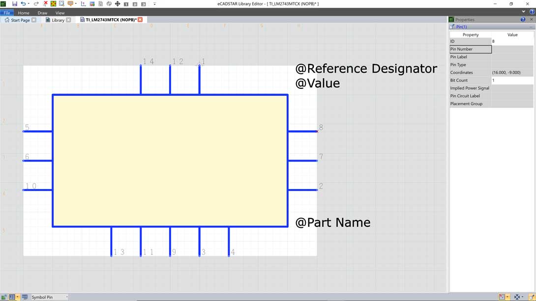
Schematic symbols often represent parts or functions within them, but they can also be items like sheet connectors, power supply voltages, and routing star points.
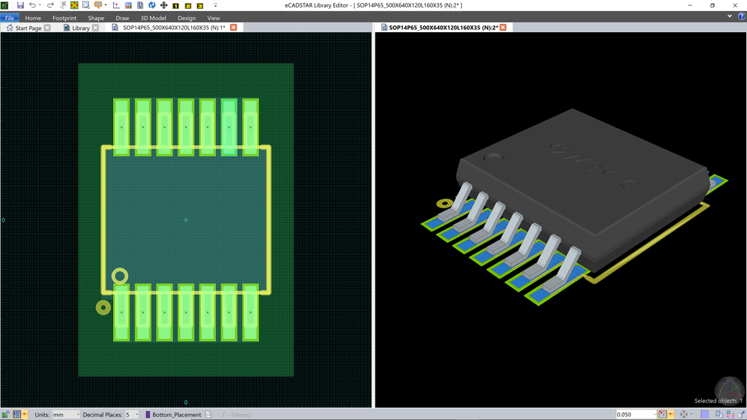
Footprints are what gets imprinted on the unpopulated PCB for a component. Pads, conductor shapes, solder mask, and any other data layers. You can include documentation layers too. Footprints can consist of 3D models. You can import STEP format models and these are often included in data for web parts.
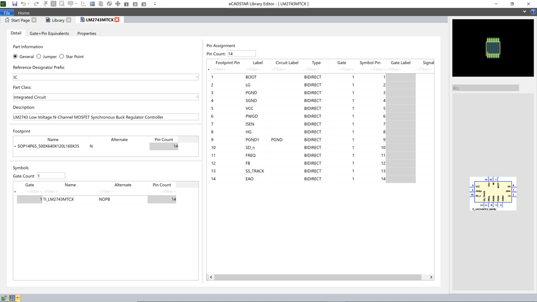
Parts unite schematic symbols and footprints, managing pin assignments and settings like legal pin swaps and the symbols used to represent each function (called “gates”, but can be items such as IO banks or multi-voltage power supply symbols).
Just as with PCB technology and design rules, these items are structured for maximum re-use and minimum repetition. You can independently create and edit pads, padstacks, footprints, the parts that use them and the symbols that represent those parts—but without switching applications.
You can download web parts and merge them directly into your library.
Once in the library they become fully editable and you can adjust them to, for example, comply with your company standards. eCADSTAR features direct integration to some of the world’s largest part vendors and online component libraries, including Allied Electronic & Automation, Arrow, Digi-Key, Mouser Electronics, RS, SamacSys and Ultra Librarian.
You can open schematic symbols, parts and footprints for editing from Library Editor’s main tab. When you edit footprints, you can even split to multiple views in any mix of 2D and 3D, to avoid later surprises due to out-of-view errors. Built-in access to cloud component libraries, including electrical schematic symbols, datasheets and 3D models makes PCB prototyping fast and accurate and you can manage part obsolescence and sourcing dynamically. With eCADSTAR’s fully-structured PCB parts libraries, you only enter data once and re-use it anywhere, bringing greater efficiency, accuracy and reliability.
3D Model Manager
The 3D Model Manager organises your 3D models to suit your standards with fantastic 3D visibility. Rename, assign or delete 3D component models and have transparency on what each 3D model represents in your library. For example, matching a corporate footprint naming convention
Even organise these models into subfolders bringing structure and clarity to 3D component models, such as organising them according to package style. You can visualize these models in 3D as you manage them.
Additionally import models from a wide range of popular 3D formats, expanding your choice of 3D model sources.
CONSTRAINT BROWSER
Setting constraints means you can verify that your design meets standards—internal or external. And your design follows those constraints as you go, because it costs much less to avoid an issue than to find and fix it later.
A constraint set early works for you, but consistency is critical. A constraint in library design rules must look the same and work the same as one applied locally, in schematic or PCB.
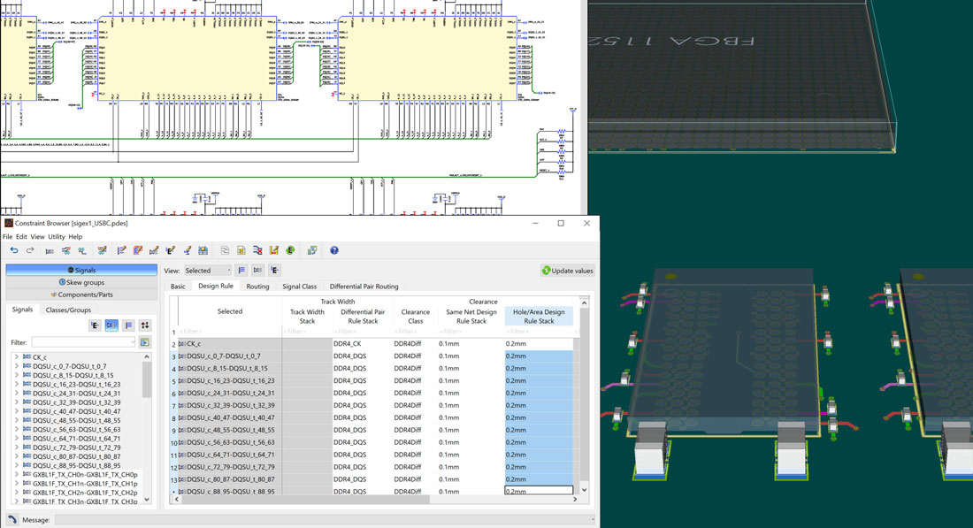
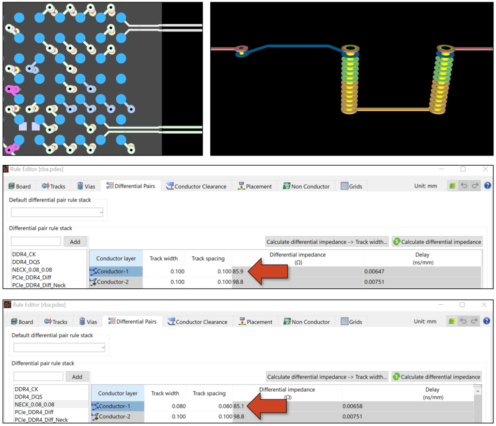
Necking-down DDR4 strobe routing by switching between differential pair rule stacks as it approaches its controller. Differential pair rule stacks defined in the library can been set as constraints using the unified Constraint Browser in both schematic and physical PCB design.Xi
Design Rule and Constraints
Set or edit constraints in Schematic Editor or PCB Editor. Define technology and design rules in Library Editor. Keep your design settings in sync with your master library or make them local.
Local settings can be useful for prototyping, while synchronized settings are best for production.
Manage constraints in Constraint Browser, in a clearly presented object hierarchy. Look and feel is the same whether you do that in Schematic Editor or PCB Editor.
Forward and back annotation ensure that your constraints are always in sync. Define classes and groups to organize your design and constraints. Create differential pairs and buses. Cross probe selections between the canvas and Constraint Browser in both Schematic Editor and PCB Editor. Highlight objects you constrain by setting colors and taking advantage of visibility options such as shading between differential +/- and E-net pin pairs.
Route with confidence, assisted by simultaneous display of real-time measurements versus constraints.
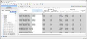
Constraint Browser showing constraints and results for differential memory strobesXi
All The Contraints You Need
With eCADSTAR you can:
-Verify compliance to physical PCB design standards like clearance and creepage rules
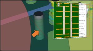
Detect inter-layer creepage paths between plane areas and copper shapes in 3DXi
-Control high-speed signal topology, impedance and skew
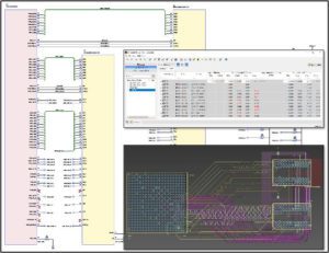
Route according to correct-by-construction topology rules and auto-lengthen for skew optimizationXi
-Verify constraint compliance with built-in, consistent simulation
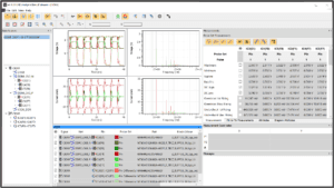
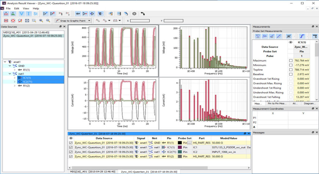
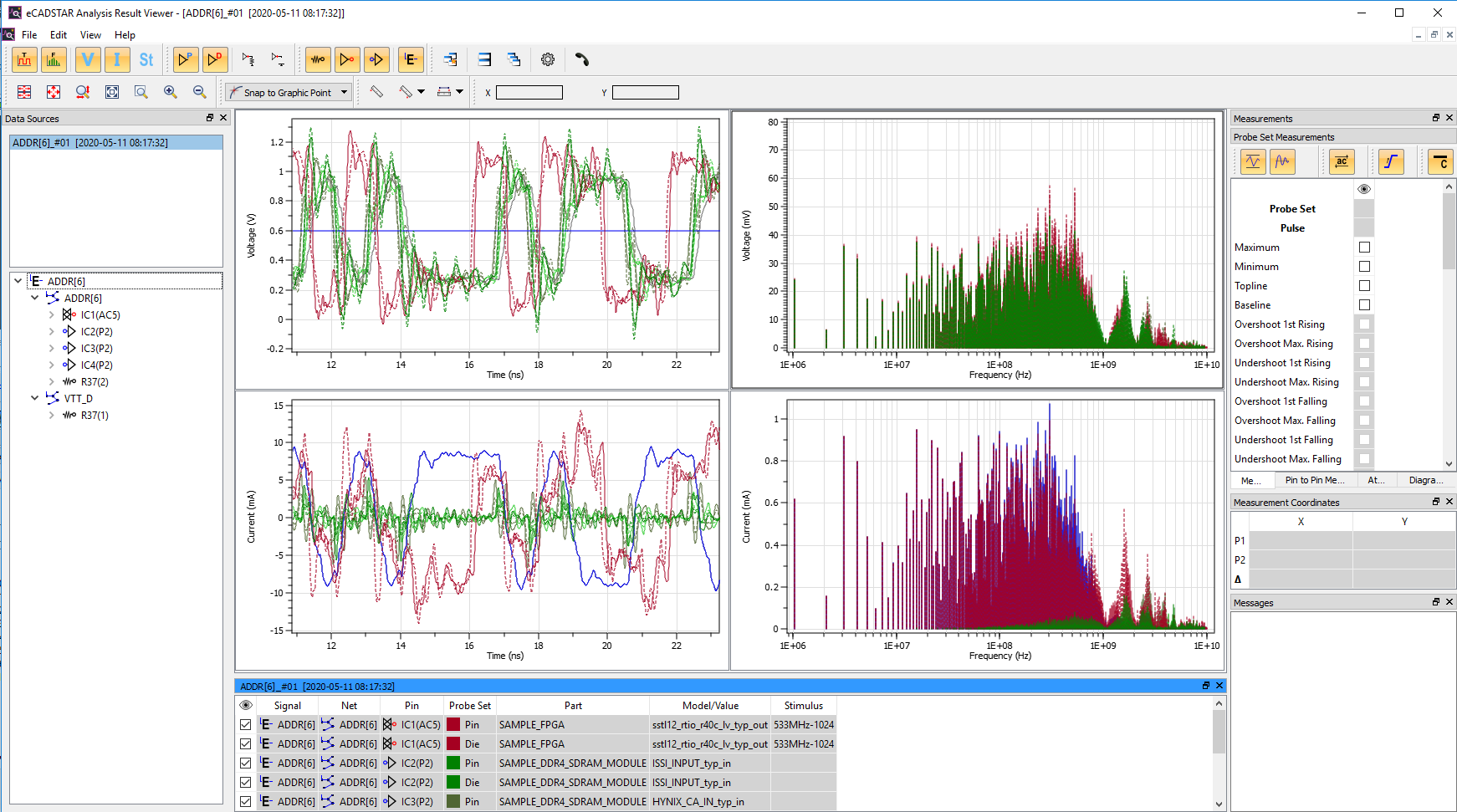
Verify signal and power integrity with time and frequency domain simulation
Drive and organize your analog simulation more effectively
In our increasingly digitized world, analog circuits show no sign of diminishing. Mixed analog/digital designs are very common. Sensors, controllers and multimedia interfaces all include analog circuits.
Traditionally, analog analysis has been separate and tackled by specialists. There’s no substitute for expertise but keeping data in a different place is never a good idea—especially when there are engineering changes or enhancements.
With Schematic Editor SPICE Controller, you can set up simulation directly and that setup stays with your schematic design.
Once you are simulating with LTspice™, there is no substitute for experience and its extensive, freely available online information. But keeping the setup with your design data and closely linked to it makes tasks like AC analysis and corner case checking parts of a joined-up process.
Best-in-class analog simulation for your PCB designs
Schematic Editor SPICE Controller provides enriched integration, as well as ideal facilities to explore design options while keeping your setup with your schematic.
-Use the leading, proven analog simulator LTspice™ while keeping key data with your eCADSTAR schematic
-The LTspice™ SPICE circuit simulation software is free to download and use
-Explore operating ranges and passive component values dynamically, even if you have not yet assigned production parts. Decide on the tolerances, wattages, etc. that you need to make your design both economical and robust
-Perform Monte Carlo analysis to check for random combined-effect issues that can put your analog circuit’s performance out of specification, without the number of simulations getting unrealistically high.
Preserve and recall settings easily with built-in simulation control
You can simulate parts of your schematic or your whole design. It is usually more useful to focus on specific circuits. LTspice™ models have their own pin numbering conventions. As well as mapping to the correct pins to simulate components like transistors, diodes and operational amplifiers, you can override the values of passive components like resistors and capacitors. You can, for example, explore the effect of different bias levels, passive filtering or alternate independent voltage sources.
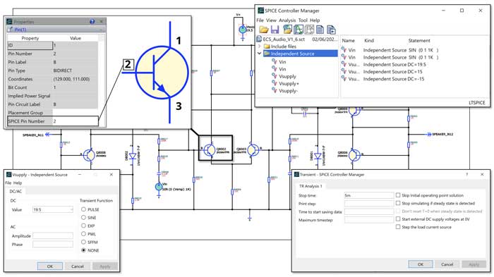
You define the simulation setup and LTspice® model pin assignments directly in Schematic Editor. This means the setup data stays safely with the design instead of being separate.
Simulate your analog circuits with powerful, industry-proven methods
Once you have set up the simulation parameters, you can save and re-use them for the same schematic. The simulation parameters are paired with the simulation netlist you generate, so they are valid only for that circuit. Once LTspice® simulation is running, you have all the facilities that it offers.
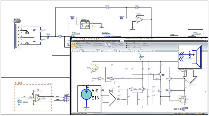
This simulation netlist is for one sheet of the schematic: an audio amplifier circuit. You can also simulate framed areas of your schematic or your whole schematic.
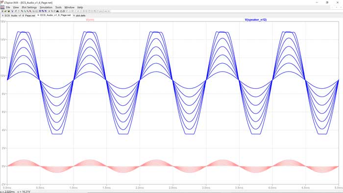
In this simulation of an audio amplifier, the lower, red traces show the amplitude of the input signal being swept in 0.1 Volt steps. The corresponding blue traces above show the response at the speaker output. You can see at what input level the output stops clipping. In audio terms, this would be the point at which a guitarist stops sounding as though they are using a fuzz box.
Roll the dice before production and beat the odds of a surprise
As its name suggests, Monte Carlo analysis is about rolling the dice. What will happen if multiple things over which we have no control vary at random and simultaneously? What if the environment is particularly hot or particularly cold and at the same time, one or more of the components is operating at the limits of its specification?
Simulating all situations where there are multiple variables means a very large number of simulations. If you roll two dice at Monte Carlo, they can land in 6×6=36 different ways. If you have, say, five variables, each in ten different states, then your number of simulations would be 10×10×10×10×10=100,000.
The beauty of Monte Carlo analysis is that instead of simulating all values, it intelligently randomizes which values to consider based on mathematical statistics.
Here is a simple example: checking the effect of a ten percent versus a one percent tolerance for the input and output resistors of an operational amplifier. You choose the number of samples and variations in the two values are distributed intelligently to show the variation in output without having to simulate every case.
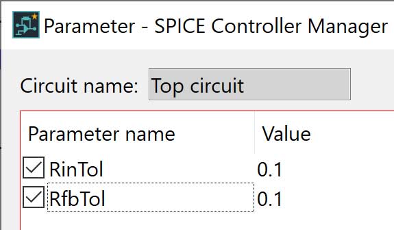
The two resistor tolerances are set by these parameters. For the first Monte Carlo simulation, they are set to 0.1, which represents a 10% tolerance.
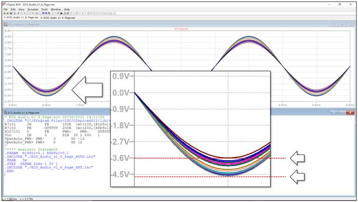
There is about a 1V drift in output amplitude as both resistors drift from their ideal values—too much for this circuit. The setup created within SPICE Controller in Schematic Editor is shown in LTspice® form in the same view.

There is about a 1V drift in output amplitude as both resistors drift from their ideal values—too much for this circuit. The setup created within SPICE Controller in Schematic Editor is shown in LTspice® form in the same view.
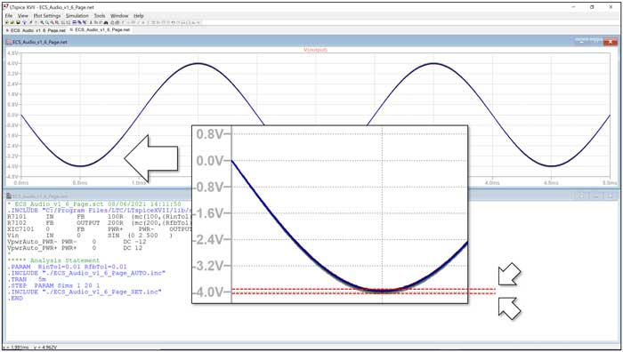
When both resistor tolerances are set to one percent, the same Monte Carlo simulation shows a very small output amplitude drift, so one percent tolerance resistors are chosen for this circuit.
What Schematic Editor’s SPICE Controller gives you and how best to use it
Why not just use LTspice® directly? You can add and connect components right there and simulate them. There is no reason why you should not do that too, but SPICE Controller keeps the simulation setup with your schematic design and links simulation to your schematic design data. That makes LTspice® simulation cases both easier to manage and easier to set up. It closes the loop between your schematic design and your LTspice®analysis in a way that means you can retrieve it later.
The recommended way, preferred by many analog engineers, is to create separate mini designs in Schematic Editor that they can use as design building blocks, together with their simulation setups. These can be imported into different schematic designs while keeping the reference copies of the analog designs separate. If an analog designer enhances one of these circuits, it will be available as an upgrade to designs that use it at a time of your choosing.
Here is a demonstration that goes deeper into LTspice® simulation from Schematic Editor
MANUFACTURING DATA & REPORT GENERATION
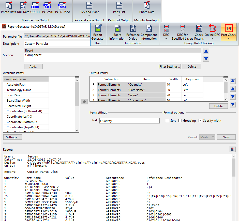
With documentation layers you can generate manufacturing information such as dimension lines, drill hole tables and scaled areas alongside your design content. With fully configurable export options, output only the layers you need.
Generate parts lists and pick-and-place reports using the built-in reporting tools. Using report templates, you can configure content and format too, including sorting, filters, sections, header/footer, and macro variables. Re-use your report templates between designs to integrate cleanly with your PLM system.
Import and export native, industry standard formats such as Photo Data (GerberX), Drill Data (Excellon2), OBD++, IPC-2581, and IPC-D-356A, to produce manufacturing-ready data.
PDF OUTPUT
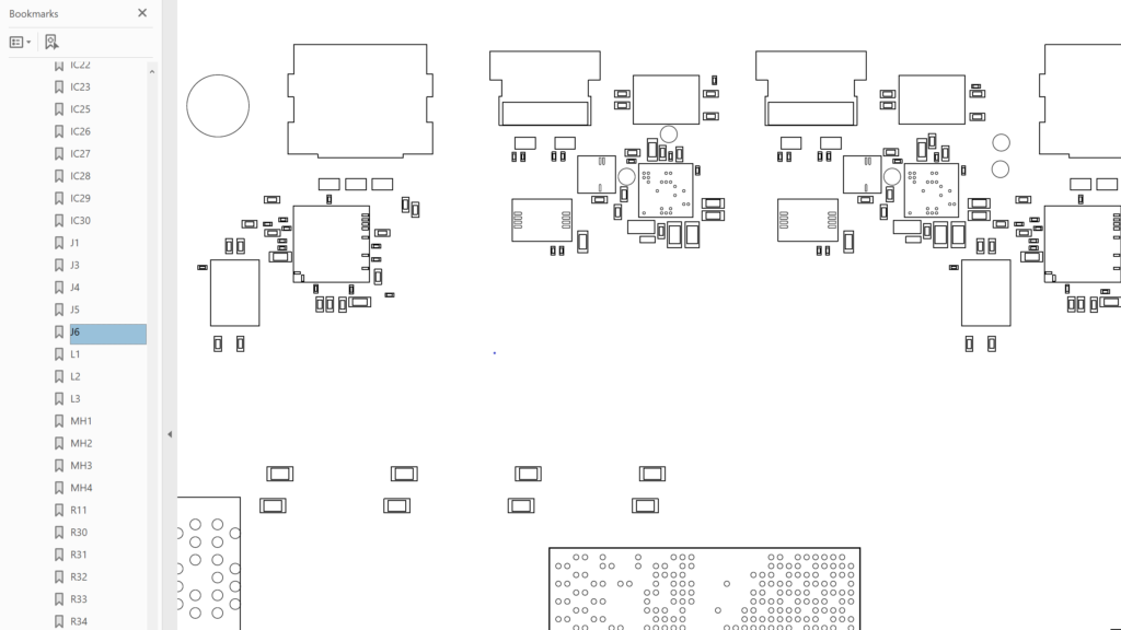
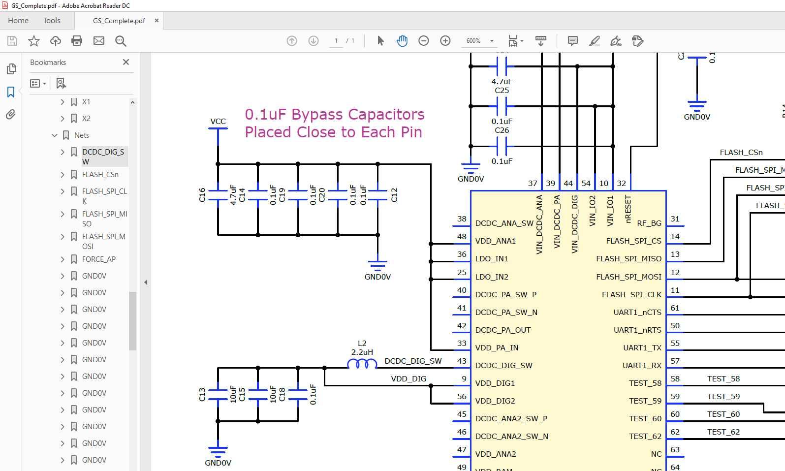
With Intelligent PDF Output, you can share as much or as little as you like, protecting the IP that makes you unique. Make detailed choices on format, layers, physical objects and areas of your design you want to share, and those you don’t. Bookmark components automatically for easier PDF interpretation.
USER SCRIPTING
Allowing you to interact with eCADSTAR via the Component Object Model (COM) interface. This means you can choose your own scripting language (PowerShell, VB, C#, C++). With scripting, you can, for example, format a report any way you like, with total flexibility.
WEB LOOKUP & PART DOWNLOAD
The same Library Searcher is built into eCADSTAR Schematic, PCB and Library Editor. Select your preferred part vendor from Allied Electronic & Automation, Arrow, Digi-Key, Mouser Electronics, PCB Libraries, RS, SamacSys, SnapEDA, SupplyFrame (FindChips) and Ultra Librarian. View live part information including stock and pricing. The selected part is downloaded directly to your library and it’s on your cursor, with just one click.
eCADSTAR features direct integration to some of the world’s largest part vendors and online component libraries. Find part information instantly, with direct access to live information. In stock? Right price? Download that part or merge it into your library. In many cases, part downloads are free.
Part information includes schematic symbol, PCB footprint and 3D model, ready to use in your designs. You can adjust these to your own standards in eCADSTAR Library Editor if you need to. Footprints that you download are automatically mapped to your specific library layers and color set, maintaining any 3D model alignment and reducing the need to edit.
WEB BOM TOOL
The eCADSTAR Web BOM Tool will run SiliconExpert SE CONNECT optimizing your design process. SiliconExpert CONNECT identifies potential risk using SE design and component libraries via our embedded service. SE CONNECT is built into eCADSTAR Schematic and PCB Editor. Upload your Bill Off Material (BOM) and run a SiliconExpert BOM analysis of the parts used within your project. From life-cycle classification and compliance information to crosses, stock levels, and pricing data, your engineers can have access to reliable data to drive their decisions and streamline design processes.
ONLINE HELP, TOOLTIPS, DASHBOARD
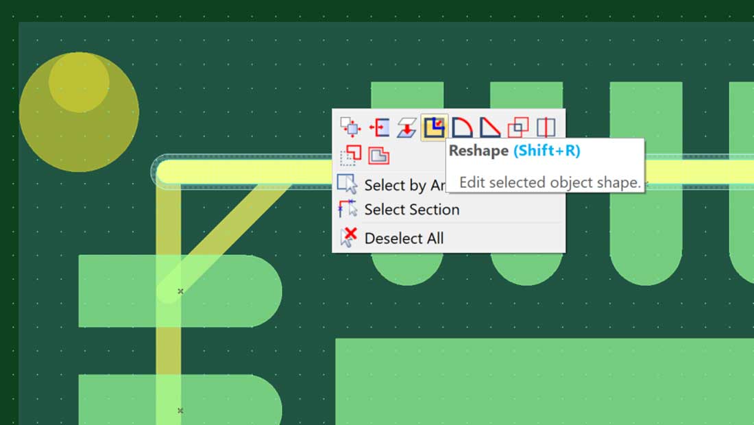
You’re always connected to the latest information for your eCADSTAR applications. Click in-context to go straight to what you need or search for broader content. If all you need is a quick reminder, just float the cursor over an item on the ribbon and a tooltip will appear. You stay in control – online, on-site or on your desk, the choice is yours. Sign in to your eCADSTAR Dashboard to enable live content and updates.
… and the eCADSTAR Dashboard is your portal to a whole lot more, including:
- Online Training
- Questions and Answers
- Our online Zuken Global Support system (ZGS), including call logging and progress updates
- Software updates
INTEGRATED ONLINE SUPPORT
Zuken Global Support (ZGS) is your online portal, linking you to a host of resources, downloadable content and live support. ZGS is provided exclusively for Zuken customers, with direct access to your local 1st line support and global 2nd line. Log questions, issues and suggestions using the Hotline logging system.
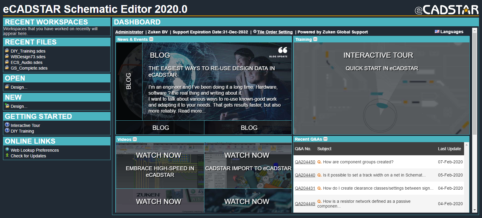
A live ZGS dashboard is displayed on the start page of each eCADSTAR application, allowing you to stay up to date with software updates, product news and hotline progress. It also provides access to live features within eCADSTAR including web lookup, part download and help content.

Free Schematic & PCB Viewers
Work seamlessly with all eCADSTAR data in one consistent, unified environment. Share your design data for free, but keep full control, with the eCADSTAR Schematic and Printed Circuit Board Design Viewers.
You do not always need a Schematic Editor or PCB Editor license to access eCADSTAR. With the free eCADSTAR Schematic and PCB Design Viewers, you can review your schematic and PCB designs without an editor license. The viewers are read-only versions of eCADSTAR Schematic Editor and PCB Editor and their user interface styles are identical.
Download the Free Viewers and Boost Your Team’s Performance
These benefits and more
- Schematic & PCB Design Viewers give you the key to unlock a seamless, consistent review process
- Schematic & PCB Design Viewers empower collaboration; consistency and freedom from extra cost reveal new opportunities for team working
- Viewers have an identical look and feel to eCADSTAR Schematic Editor and PCB Editor, so there is no additional learning curve for staff and other design team workers
- Viewers introduce no extra data formats, maximizing interoperability and minimizing additional data management
Free Schematic and PCB Design Viewers for Seamless Design Reviews
When you design your products in eCADSTAR, would you like to share your Schematic and PCB Design files with your teams, both internal and external? Do you have to protect your work by granting read-only access to be sure there will be no unexpected edits? Our free Schematic and PCB viewers read the same eCADSTAR file formats (*.sdes and *.pdes) as Schematic and PCB Editors.
Your data is presented in a unified environment that is accessible to every member of your team. With eCADSTAR Schematic and PCB Design Viewer, your audience can access, read, review, track progress and share your EDA designs. With over 40 years’ experience in the PCB design software industry and utilizing the latest Zuken technology, the realities of electrical and electronic engineering design are well-known to us. They are central to everything we do.
And the best part is, there is no need to purchase an eCADSTAR software license. Sign-up for your own Free eCADSTAR Schematic & PCB Design Viewer.
- Check out your schematic circuits.
- Check out your part selection.
- Check out your manual routing, autorouting results, differential routing.
- Check your placement and rule areas.
- Check it out in 2D.
- Check it out in 3D. Is it right? Is it the best it can be? Make sure before you move on.
Viewers introduce no extra data formats, maximizing interoperability and minimizing additional data management
You can share data outside your organization with those who need to see it. Not having eCADSTAR PCB Editor or Schematic Editor licenses does not stop them viewing design data you give them. Of course, their access with the viewers is read-only – ideal for working with OEMs and a lot safer.
You can keep your customers informed of progress whenever you choose. Visibility means dynamic working. Observing, optimizing, noticing opportunities for re-use and spin-offs. Identifying opportunities for future collaboration.
Read-only access does not mean just a plain snapshot. The viewers include rich capabilities – a subset of those in the full editors. You can cross-probe between schematic and PCB designs. You have a full set of graphical controls including touchscreen – ideal for group reviews. You can view constraints set by engineers in schematic or PCB. You can review placement, routing and design rules with others on your team and do the same with external teams. All the time, read-only access to your data eliminates the risk of unintended changes.
Search components and nets in either eCADSTAR Schematic Viewer or PCB Viewer and cross-probe from one to the other. Or navigate in Constraint Viewer (a read-only version of Constraint Browser in eCADSTAR Schematic Editor and PCB Editor).
Review and Share all This and More With Schematic Viewer
Connectivity, including power and differential signals • All the part and net properties you need to check • Parts list/Bill of Materials/BOM • Basic constraints set by engineers and PCB designers.

Have company standards been met? Are circuit styles consistent with similar designs? Has anything been re-designed when already available elsewhere? Have all the right properties been set? Have the right units been used? Are part names, etc. in the correct format? Can collaborators help you to identify alternative part sources to identify cost reductions? Do other designers think your constraints could be too tight or too loose? Can you leverage their experience to make the journey to production smoother?
Review and Share all This and More With PCB Viewer
Complete PCB layout with full control of displayed layers and objects • Design rules, including settings like clearances, width/spacing rule stacks and via setups • PCB technology (layer stack) including materials, dielectric constants, loss tangents and thicknesses • Constraints set by engineers in logical or physical design

What you see is what the PCB designer sees; one observer can catch an issue that another misses, especially if they have manufacturing experience. Have design rules branched off from standards? If so, why? Do standards need revising or can the existing standards be applied? Has everything been understood by all concerned? Does the layer stack look right? Is there accidental asymmetry? What kinds of vias will best balance cost and performance? How about prepreg and laminate layer choices? Are they in line with impedance tolerances? How about those differential widths and spacings? Impedance looks right, but what about manufacturing? Does your process support such narrow tracks and gaps on those layers?
The Viewers are Free – You Have Nothing to Lose
eCADSTAR Schematic and PCB viewers transform design reviews with big real-world insights and savings. Turbo-charge and streamline teamworking. Make eCADSTAR Schematic Viewer and eCADSTAR PCB Viewer part of your eCADSTAR solution.
MANUFACTURING DATA & REPORT GENERATION
With documentation layers you can generate manufacturing information such as dimension lines, drill hole tables and scaled areas alongside your design content. With fully configurable export options, output only the layers you need.
Generate parts lists and pick-and-place reports using the built-in reporting tools. Using report templates, you can configure content and format too, including sorting, filters, sections, header/footer, and macro variables. Re-use your report templates between designs to integrate cleanly with your PLM system.
Import and export native, industry standard formats such as Photo Data (GerberX), Drill Data (Excellon2), OBD++, IPC-2581, and IPC-D-356A, to produce manufacturing-ready data.
PDF OUTPUT
With Intelligent PDF Output, you can share as much or as little as you like, protecting the IP that makes you unique. Make detailed choices on format, layers, physical objects and areas of your design you want to share, and those you don’t. Bookmark components automatically for easier PDF interpretation.
USER SCRIPTING
Allowing you to interact with eCADSTAR via the Component Object Model (COM) interface. This means you can choose your own scripting language (PowerShell, VB, C#, C++). With scripting, you can, for example, format a report any way you like, with total flexibility.
Creating variant designs allows components, or groups of components, to have properties such as fitted status and part to be changed within the same design. Using the variant selector, users can switch their active design canvas instantly.
Features
Simple and Complex
Using variation manager, variation structures can be quickly defined, depending on your requirement, simple mode provides users the ability to set a unique set of properties, per component, for each variant. In advanced mode users may establish variation types, reusing defined properties at a group level rather than individually.
Component Browser – Variants
The Component Browser is a global dialog that can be accessed from within Schematic Editor, it provides an abstract view of all components within your schematic design. Apply searches and filters to distinguish between components and modify a range of properties either singularly or on mass. Use Component Browser to define variants and modify all variant iterations, both simple and advanced, within a single view. Quickly cross probe from the component browser to a components exact location by double-clicking within the dialog.
MANUFACTURING DATA & REPORT GENERATION
With documentation layers you can generate manufacturing information such as dimension lines, drill hole tables and scaled areas alongside your design content. With fully configurable export options, output only the layers you need.
Generate parts lists and pick-and-place reports using the built-in reporting tools. Using report templates, you can configure content and format too, including sorting, filters, sections, header/footer, and macro variables. Re-use your report templates between designs to integrate cleanly with your PLM system.
Import and export native, industry standard formats such as Photo Data (GerberX), Drill Data (Excellon2), OBD++, IPC-2581, and IPC-D-356A, to produce manufacturing-ready data.
PDF OUTPUT
With Intelligent PDF Output, you can share as much or as little as you like, protecting the IP that makes you unique. Make detailed choices on format, layers, physical objects and areas of your design you want to share, and those you don’t. Bookmark components automatically for easier PDF interpretation.
USER SCRIPTING
Allowing you to interact with eCADSTAR via the Component Object Model (COM) interface. This means you can choose your own scripting language (PowerShell, VB, C#, C++). With scripting, you can, for example, format a report any way you like, with total flexibility.
INCREASED PRODUCTIVITY
Release 2020 eCADSTAR, Zuken’s internet connected PCB design platform has been extended to include new optional modules for signal integrity, power integrity, IBIS-AMI simulation and much more.
SIGNAL INTEGRITY
Embedded Signal Integrity simulation in Schematic and PCB Editors for pre- and post-layout simulation.
SIGNAL INTEGRITY ADVANCED
Builds on the functionality that the Signal Integrity option delivers and adds even more functionality for very high speed design.
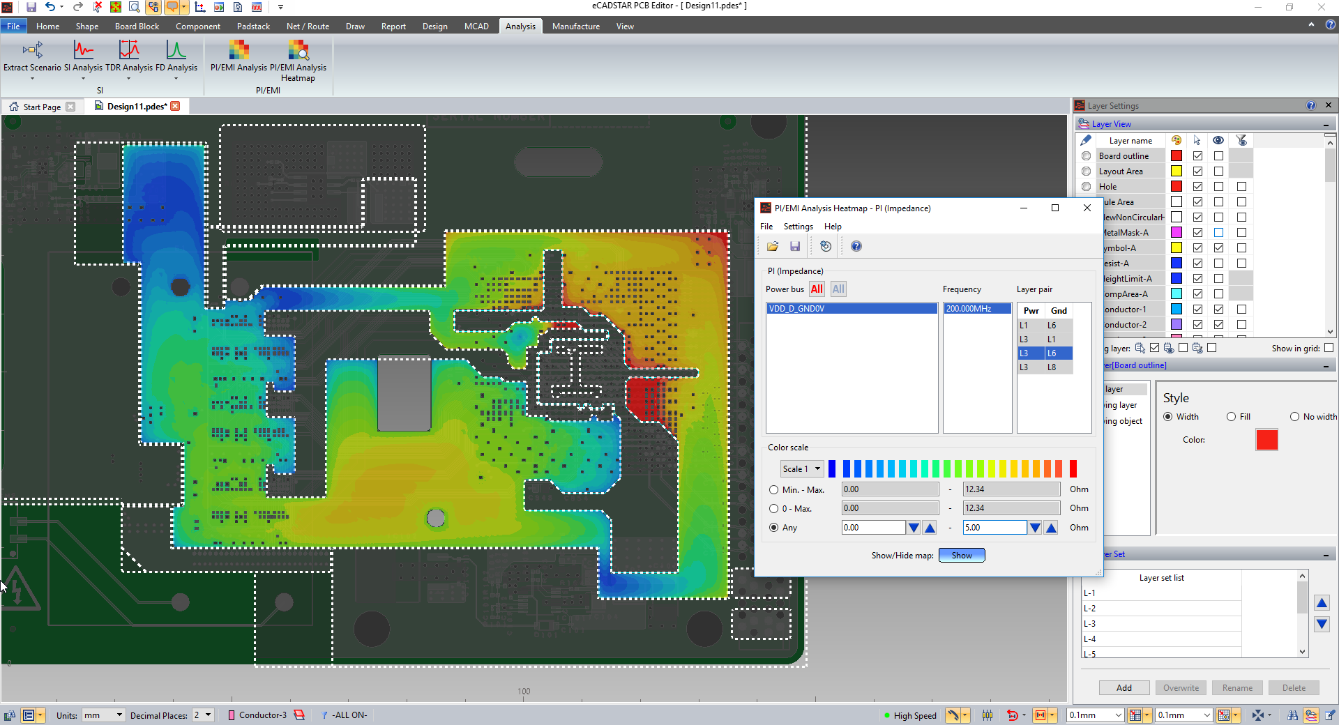
POWER INTEGRITY AND EMI ANALYSIS
Embedded Power Integrity and EMI Analysis to optimize EM compliance and performance.
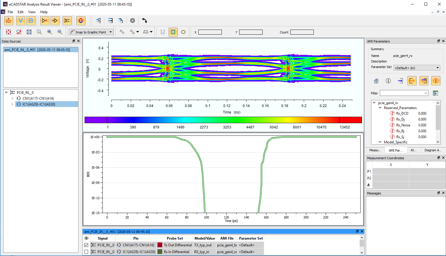
IBIS-AMI
Adding sophisticated IBIS-AMI Analysis capabilities to the eCADSTAR SI Simulation modules.
TOPOLOGY DRIVEN ROUTING
Route topologies with Virtual Branch Points (VBPs) as a guide.
ENHANCED DASHBOARD
Increased usability and online help improvements.
INTELLIGENT PDF OUTPUT
Customise which properties and create bookmarks for easy navigation.
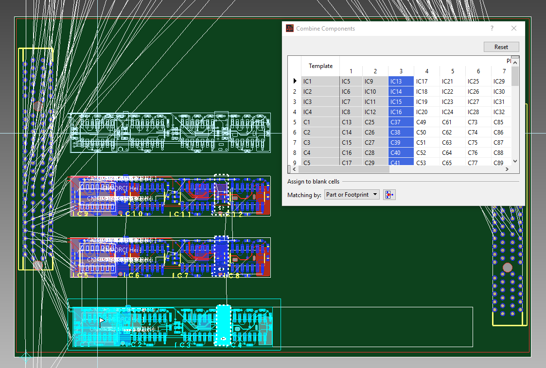
COPY PLACEMENT IN PCB EDITOR
Replicate easily and quick one channel placement and routing to other unplaced channels.
PCB Layout Proven, Professional, Comprehensive Results
The PCB design Editor is eCADSTAR’s PCB layout application, a key part of our unified, internet-connected EDA solution. eCADSTAR applications are clear and consistent. You work quickly and correctly. One user interface style. Universal web connectivity. Industry-proven technology. A short learning curve, but all the detailed features you need to optimize your designs.
Give Your PCB Designers What They Need
- Instant web and local parts—prototype at full speed with library admin control when you need it
- Simultaneous, native 2D/3D with mechanical design integration—design and visualize in ways that suit you
- Block hierarchy—give your design structure and benefit from efficient re-use, including inter-team sharing
- Superb interactive placement and routing—optimize your critical circuits
- High-speed—control impedance and topology
- Autorouting—save time and make eCADSTAR work for you
- Range of manufacturing outputs and inputs—optimize interaction with fabricators
- Rules By Area
- 3D Creepage Check
Instant Web and Local Parts
Save time when you prototype, even before your new components are in your library. Download what you need and carry on working. Search for a part and it appears on your cursor. Drop it and it becomes part of your PCB layout.
Web part lookup gives PCB engineers access to extensive online parts libraries, including 3D models.
Native 3D and Simultaneous 2D/3D PCB Design
2D or 3D viewing—which is best? To avoid DRCs while placing components, usually 3D PCB design. And with fast signalling, the third dimension really comes into play. But when you’re routing, working in 2D provides more focus on routing topology and patterns. So why choose when you can have both? You can split the view and route in 2D with simultaneous 3D display.
Additionally, your 3D canvas can include both PCB and enclosures. You get ahead, detecting issues like component-to-enclosure collisions right on the canvas.
Native 3D design means collisions and DRCs get detected early—often in real-time, during interactive layout. Another great feature is simultaneous 2D/3D design. It gives you the best of both worlds—for example routing a critical differential pair in a familiar 2D view while seeing how it relates to other objects in 3D.
Board Blocks
Board Blocks equip you for maximum re-use, design integrity and teamwork. Once you create a block and make it a child board, you can re-use it anywhere on your PCB design. Furthermore, you can work on blocks independently and merge or re-merge them intelligently into your designs. You can even create your own library of physical design blocks and share with whoever you wish.
Board Blocks are parts of a PCB design that you identify and save as re-usable work. If you identify a Board Block as a Child Board, then you can re-import it at any time to reflect engineering changes (ECOs)—even if other engineers have worked on it. For example, you may have a colleague who is particularly good at optimizing power supply layout, so you can re-import later without interrupting your work on the main PCB design.
Design PCBs With Superb Interactive Routing
At the heart of PCB design Editor is its highly configurable yet straightforward interactive routing. eCADSTAR recognizes that signals take many forms and our PCB layout platform works with you to get them connected as neatly and effectively as possible, considering all the intricacies of today’s PCBs.
Denser and denser routing carrying faster and faster signals with more and more mixing of analog, digital, power, and RF. Our PCB design Editor was designed to handle all that, with the help of your skill and experience.
Optimize PCB layout with efficient interactive routing with control where you need it. Interactive routing follows guidelines you can configure, helping you conform to best practices.
High-Speed Design
With our PCB design Editor, high-speed design is built-in, not an afterthought. It goes as shallow or as deep as you need. Yes, topology control, impedance control, simulation and power integrity analysis when you need them, but advanced re-use features also make high-speed design much faster and safer.
Some high-speed features are cost options, so you decide and pay for only what you need.
Control high-speed layout without external software in a consistent, unified environment: Topology, impedance, crosstalk, signal integrity and much more.
Design PCBs Using Autorouting
Autorouting has come a long way since the days of join-the-dots when designing a PCB. What you can achieve depends on the kind of design you have and the parts of the design you want to route with it. This requires a detailed routing strategy. A good strategy requires some expert assistance, and this is where the eCADSTAR Routing Consultant comes into play.
Some PCB circuits are good candidates for autorouting, including controllers surrounded by interface or other components and fan-out. Autorouting requires a strategy. That is where the autorouting in eCADSTAR’s PCB design Editor excels. Routing Consultant creates a basic strategy that you can adjust to perfection, apply, and save for future use.
Range of Manufacturing Inputs and Outputs
A good range of manufacturing outputs means you give fabricators what they need for fast and accurate turnaround. Gerber import lets you add legacy and external artworks to your designs, with intelligent data merge.
You can supplement manufacturing and review data with fully-customizable reports, including details of physical board, components, pins, padstacks and holes.
The range of manufacturing outputs in PCB Editor means you can supply data in the best form for each recipient. Gerber data import is intelligent—much more than mere artwork import—so it’s easier to re-use external and legacy data when Gerber is all you have.
Rules by Area
Create rule areas on your PCB – as many as you like and any shape. Assign both single-ended and differential rule stacks to them, with the further option to refine by PCB layer.
As well as automatically necking-down tracks and differential pairs in high-density areas, you can localize via rules to help control cost and reliability – for example, specifying HDI via types and spans only in places they are needed.
3D Creepage Checks For Your PCB Design
eCADSTAR Advanced 3D and Ultimate only
External variables that are hard to control, like industrial pollution and humidity, can create paths on insulators that current “creeps” over. The higher the voltage, the more likely this becomes. Unforeseen creepage causes both safety and reliability issues.
PCB Layout Proven, Professional, Comprehensive Results
The PCB design Editor is eCADSTAR’s PCB layout application, a key part of our unified, internet-connected EDA solution. eCADSTAR applications are clear and consistent. You work quickly and correctly. One user interface style. Universal web connectivity. Industry-proven technology. A short learning curve, but all the detailed features you need to optimize your designs.
Give Your PCB Designers What They Need
- Instant web and local parts—prototype at full speed with library admin control when you need it
- Simultaneous, native 2D/3D with mechanical design integration—design and visualize in ways that suit you
- Block hierarchy—give your design structure and benefit from efficient re-use, including inter-team sharing
- Superb interactive placement and routing—optimize your critical circuits
- High-speed—control impedance and topology
- Autorouting—save time and make eCADSTAR work for you
- Range of manufacturing outputs and inputs—optimize interaction with fabricators
- Rules By Area
- 3D Creepage Check
Instant Web and Local Parts
Save time when you prototype, even before your new components are in your library. Download what you need and carry on working. Search for a part and it appears on your cursor. Drop it and it becomes part of your PCB layout.
Web part lookup gives PCB engineers access to extensive online parts libraries, including 3D models.
Native 3D and Simultaneous 2D/3D PCB Design
2D or 3D viewing—which is best? To avoid DRCs while placing components, usually 3D PCB design. And with fast signalling, the third dimension really comes into play. But when you’re routing, working in 2D provides more focus on routing topology and patterns. So why choose when you can have both? You can split the view and route in 2D with simultaneous 3D display.
Additionally, your 3D canvas can include both PCB and enclosures. You get ahead, detecting issues like component-to-enclosure collisions right on the canvas.
Native 3D design means collisions and DRCs get detected early—often in real-time, during interactive layout. Another great feature is simultaneous 2D/3D design. It gives you the best of both worlds—for example routing a critical differential pair in a familiar 2D view while seeing how it relates to other objects in 3D.
Board Blocks
Board Blocks equip you for maximum re-use, design integrity and teamwork. Once you create a block and make it a child board, you can re-use it anywhere on your PCB design. Furthermore, you can work on blocks independently and merge or re-merge them intelligently into your designs. You can even create your own library of physical design blocks and share with whoever you wish.
Board Blocks are parts of a PCB design that you identify and save as re-usable work. If you identify a Board Block as a Child Board, then you can re-import it at any time to reflect engineering changes (ECOs)—even if other engineers have worked on it. For example, you may have a colleague who is particularly good at optimizing power supply layout, so you can re-import later without interrupting your work on the main PCB design.
Design PCBs With Superb Interactive Routing
At the heart of PCB design Editor is its highly configurable yet straightforward interactive routing. eCADSTAR recognizes that signals take many forms and our PCB layout platform works with you to get them connected as neatly and effectively as possible, considering all the intricacies of today’s PCBs.
Denser and denser routing carrying faster and faster signals with more and more mixing of analog, digital, power, and RF. Our PCB design Editor was designed to handle all that, with the help of your skill and experience.
Optimize PCB layout with efficient interactive routing with control where you need it. Interactive routing follows guidelines you can configure, helping you conform to best practices.
High-Speed Design
With our PCB design Editor, high-speed design is built-in, not an afterthought. It goes as shallow or as deep as you need. Yes, topology control, impedance control, simulation and power integrity analysis when you need them, but advanced re-use features also make high-speed design much faster and safer.
Some high-speed features are cost options, so you decide and pay for only what you need.
Control high-speed layout without external software in a consistent, unified environment: Topology, impedance, crosstalk, signal integrity and much more.
Design PCBs Using Autorouting
Autorouting has come a long way since the days of join-the-dots when designing a PCB. What you can achieve depends on the kind of design you have and the parts of the design you want to route with it. This requires a detailed routing strategy. A good strategy requires some expert assistance, and this is where the eCADSTAR Routing Consultant comes into play.
Some PCB circuits are good candidates for autorouting, including controllers surrounded by interface or other components and fan-out. Autorouting requires a strategy. That is where the autorouting in eCADSTAR’s PCB design Editor excels. Routing Consultant creates a basic strategy that you can adjust to perfection, apply, and save for future use.
Range of Manufacturing Inputs and Outputs
A good range of manufacturing outputs means you give fabricators what they need for fast and accurate turnaround. Gerber import lets you add legacy and external artworks to your designs, with intelligent data merge.
You can supplement manufacturing and review data with fully-customizable reports, including details of physical board, components, pins, padstacks and holes.
The range of manufacturing outputs in PCB Editor means you can supply data in the best form for each recipient. Gerber data import is intelligent—much more than mere artwork import—so it’s easier to re-use external and legacy data when Gerber is all you have.
Rules by Area
Create rule areas on your PCB – as many as you like and any shape. Assign both single-ended and differential rule stacks to them, with the further option to refine by PCB layer.
As well as automatically necking-down tracks and differential pairs in high-density areas, you can localize via rules to help control cost and reliability – for example, specifying HDI via types and spans only in places they are needed.

3D Creepage Checks For Your PCB Design
eCADSTAR Advanced 3D and Ultimate only
External variables that are hard to control, like industrial pollution and humidity, can create paths on insulators that current “creeps” over. The higher the voltage, the more likely this becomes. Unforeseen creepage causes both safety and reliability issues.

EMBRACE HIGH-SPEED DESIGN WITH CONFIDENCE
With its highest performing routing tool, eCADSTAR offers specific functionality targeted for high-speed PCB design, such as DDR2, DDR3, DDR4 and PCI Express, including min/max length, skew, delay and crosstalk limits to meet tight timing and noise margins.
Overlooking a high-speed circuit creates signal chaos
You have to design the routing topology of your high-speed PCB carefully—trace geometry, layer stack, materials and electromagnetic coupling—or else signals will be degraded or dysfunctional.
This can apply to any part of a circuit board. Many standards, including the commonest memory circuits, PCI Express and USB, require high-speed PCB layout and routing.
Selected areas—or even signal layers—of a PCB, often must be treated as high-speed, even if the rest of the PCB does not.
High-speed design means concern for signal integrity. Treating high-speed signals as travelling waves. Making the paths they take as smooth as possible in electrical, not just physical, terms. You can optimize your PCB design for maximum resilience, going beyond basic design rules and guidelines such as trace length, trace width, and component placement.
Design epic high-speed PCBs with minimum setup
eCADSTAR offers specific features for high-speed PCB design, such as DDR3, DDR4, and PCI Express. These include topology, min/max length, skew, delay and crosstalk limits to meet tight timing and noise margins. But you do not always need constraints to make progress. eCADSTAR works with you to get real-world results in the quickest possible way. For example, you can:
-Copy relative placement or routing between similar channels and share it with other designers, eliminating reimplementation errors and making design upgrades much easier and more consistent
-Automatically match node-to-node lengths with no need to set constraints—a real timesaver for matched signals such as byte lanes and address/command buses
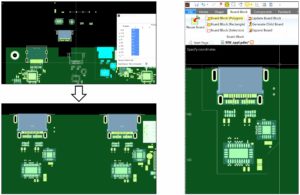
Figure 1: Placement replication on a second high-speed port
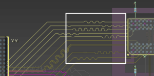
Figure 2: Automatic, no-constraint, node-to-node length matching for a DDR4 byte lane
Quick, accurate, on-cursor high-speed topology control
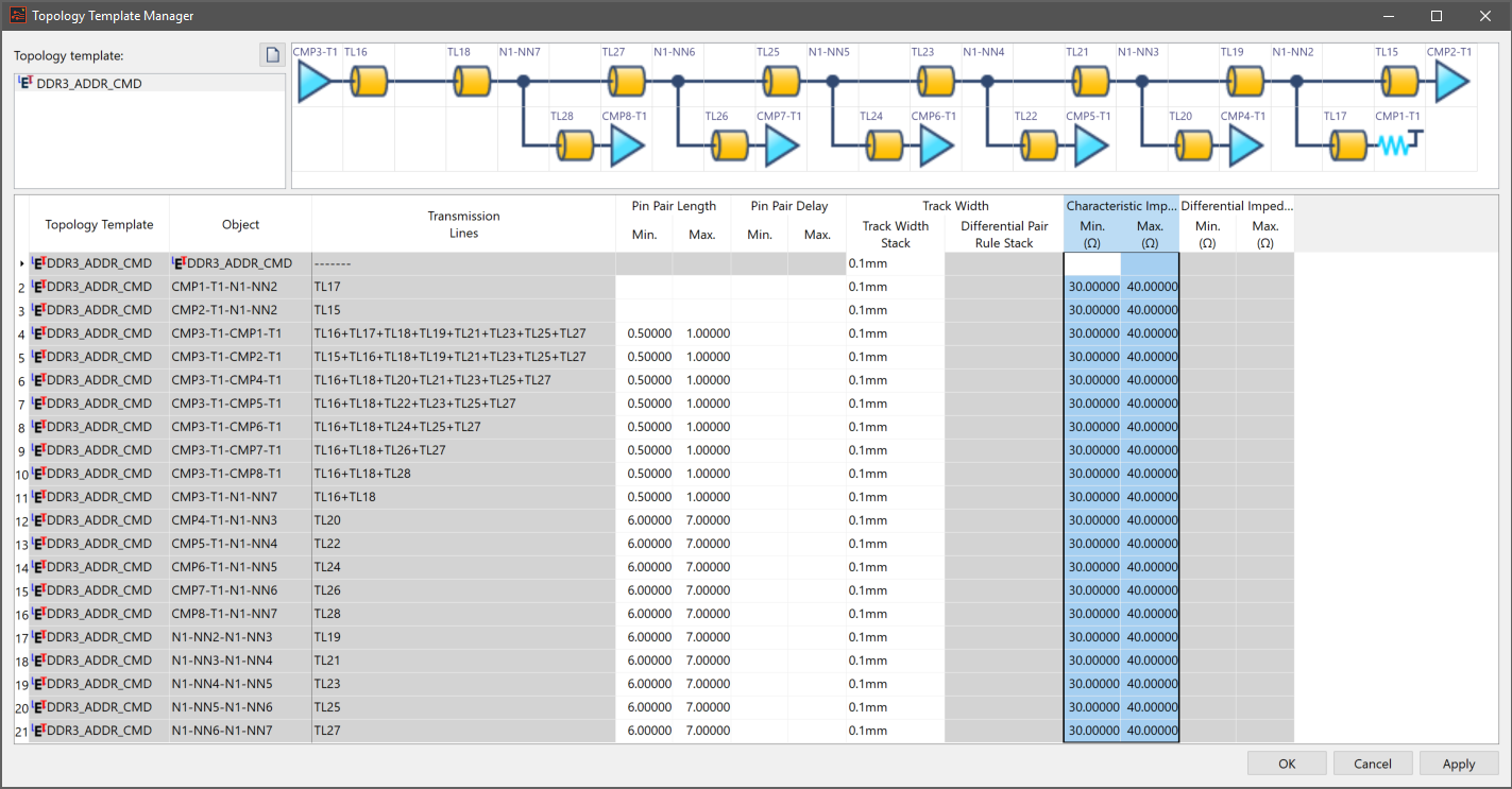
Set up standard topologies like “Fly-by” quickly and easily in eCADSTAR PCB Editor. Choose from a wide selection of built-in topology templates with instant visualization. And route with Virtual Branch Points as a guide.
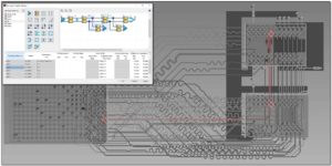
Figure 3: Topology template with constraints, applied to a DDR4 differential clock, contrasting with lowlight view in PCB Editor
Set constraints, design to them, analyze, verify—just one GUI style
Constraints serve two main purposes: checking that your design conforms to them and designing with them for correct-by-construction. eCADSTAR works with you, whatever your approach. Maybe you want to set constraints in the schematic, where you can see what the circuit is doing. Maybe you want to do that during PCB design. Constraint Browser is built into both eCADSTAR Schematic Editor and PCB Editor and the user interface is the same.
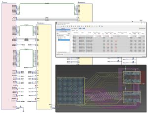
Figure 4: Minor relative length differences shown in Constraint Browser for a DDR4 bus
Control length, delay, and skew—and you don’t always need constraints
With standards-based buses such as DDR4 and PCI Express, there’s no leeway to scatter vias amongst buses at random. Length-based constraints are often the best way to route, keeping length differences (skew) very small or zero and/or keeping absolute length within tight margins.
You can set constraints in terms of delay too. This works well if application notes express constraints like that, or if the path from source to load isn’t uniform. You can combine automatic lengthening to constraints with no-constraint node-to-node lengthening. That can be more efficient – for instance matching DQ byte lanes and ADDRESS/CMD signals without constraints, before lengthening differential CK and DQS signals relative to them, controlled by constraints.
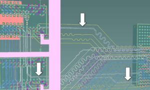
Figure 5: Clock and strobe signals, indicated by the arrows, can be lengthened to relative skew constraints after associated buses have been length-matched
Analyze, simulate and verify with best-in-class consistency
Choose what you need from the large range of simulation and analysis features in eCADSTAR bundles. High-speed simulation GUI style is consistent throughout eCADSTAR. Set up design scenarios before even starting physical design and see how they compare after placement, routing, and detailed component choice.
Include Power Integrity/EMI simulation to check DC and AC power distribution in detail and optimize critical design features like plane geometry and decoupling.
Or you can include the SPICE simulation interface, driving industry-standard LTspiceTM to simulate analog circuits directly from your design data.
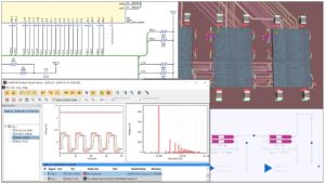
Figure 6: Consistent constraints, analysis and results
Control single-ended and differential impedance
Single-ended and differential impedance control are fundamental to high-speed design, even if constraints only apply to selected PCB areas.
eCADSTAR automatically derives widths and spacings to meet your impedance constraints, but if you prefer, you can set those directly. You may decide to do that to match a PCB manufacturer’s recommendations instead of calculating value PCB manufacturer’s recommendations can be stored in your technology and design rule shared with other designers and re-used in future designs.
What is PCB creepage and why worry about it?
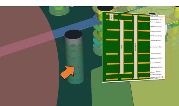
2D clearance is always less than or equal to 3D clearance. Working to 3D creepage rules means you can design more densely because clearance is measured by its true path. As well as lengthening a creepage path, a slot or hole can create an additional one in the third dimension as it is does here.
Creepage vs clearance
Clearance is the distance between objects from point to point, in 2D or 3D. The difference with a creepage check is that it considers the 3D path across the PCB. You can think of this as the terrain. Imagine a traveller walking between two villages. If they measure the distance on their map in a straight line with a ruler, that’s the clearance distance. But if there is a valley or mountain between the two villages, the distance the traveller walks will be longer than the clearance. That distance is like the creepage distance. Creepage distance is important, because sometimes you can increase the travel distance between two objects without having to move those objects further apart.
Creepage is the leakage of electrical current across the surface of an insulator.
There are two main things that make a creepage issue more likely:
- High voltage difference between two objects.
- Pollution/contaminants.
The creepage check has to know the voltage differences between objects on the PCB. For DC, you can set the voltage on each object and the voltage difference is based on the difference between those two values.

With AC signals, you have to consider relative phase.
Contaminants and pollution affect current leakage across surfaces and so expected environment is an important consideration. A damp surface is more prone to leakage than a dry one. Maybe the PCB is close to machinery and prone to vapor or oil misting.
Creepage is an important consideration in high-voltage PCB design guidelines—often applied to much higher voltage differences than the example illustrated here. Hundreds or thousands of volts. In such PCBs, although many more subtle PCB features come into play, a solid 3D creepage check is a good baseline.
Setting up useful and meaningful creepage checks
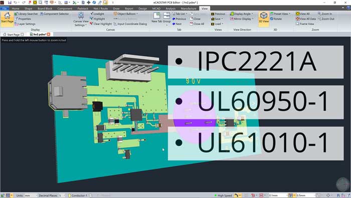
Clearance and creepage standards like IPC2221A, UL609050-1, UL-61010-1 and the more recent IEC 62368-1 (superseding 60950-1 and 60065), are graded according to defined pollution levels and cover many topics related to PCB design safety.
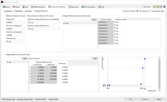
You can apply standards by defining them as Voltage Difference Clearance Tables.
You can enter rules that represent published standards as Voltage Difference Clearance Tables as well as defining your own for in-company standards.
You can include layer-dependent rules and AC phase groups. You can share voltage difference clearance rules with other engineers, independent of other design rules.
Voltage Difference Clearance Table Stacks can include layer-dependent rules.
You can set creepage rules in your master library or local design rules. You can apply them in a hierarchy. Constraint levels include whole board, differential pair class, differential pair, E-net class, E-net, net class, (logical) net and rule area.

You can apply creepage rules where you need them and not elsewhere, with the choice of applying the strictest rule or the one in the highest-priority position in the hierarchy.
Use results to dynamically optimize electrical safety and layout density
Once you have set of creepage rules, you can check objects for creepage. Checking for creepage in 3D gives you two major advantages:
- You can check effectiveness of 3D elements like slots to break or lengthen creepage paths, meaning you can pack components more densely.
- You can check for unexpected Z-axis creepage paths through the PCB created by holes and slots.
When you check creepage, you can choose a Modelling Accuracy level. Higher modelling accuracy provides more detailed analysis and takes longer. Creepage checks are made from selected objects. A typical selection would be a high-voltage bias or power signal. Search Distance is the maximum distance from those selected objects to be considered by the creepage check. The check reports creepage distances that are OK according to the rules you set as well as those that are in error. A larger Search Distance increases the time taken to generate the report. You might set Search Distance to twice or three times the minimum allowed clearance.
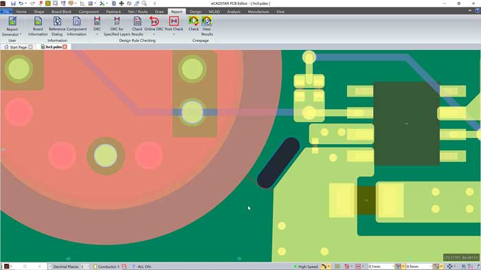
he circular shape is a 90V avalanche diode bias signal for a LIDAR system. This has to be kept clear of the nearby -5V supply, but space is tight. The length of the 3D creepage path has been increased by adding a slot, instead of increasing clearance in the horizontal plane. On the first attempt, the slot is not quite in the right position, so the creepage check fails. A red line is displayed on the PCB Editor canvas, showing the creepage path.
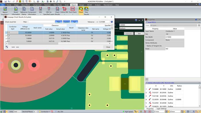
After moving the slot, the creepage path is long enough to pass the check, but a white line still displays the path to allow further optimization.
More detail in the below video
What is Gerber Import?
Gerber data describes PCB artworks, including conductors, solder masks, and drill data. Whatever other data you have, this format is the bottom line for fabrication, and it is usually available for reference design data.
The beauty of Gerber import in eCADSTAR is the way it seamlessly and intelligently merges artworks with your PCB designs. Gerber data is instantly transformed into intelligent eCADSTAR design data. Shapes become tracks and pads. Nets are automatically assigned as you place components. You can even add components and nets in PCB Editor and back-annotate the connectivity to your schematic. The choice is yours.
Many reference circuits are available in Gerber format, like this DC-to-DC Buck Regulator circuit. These circuits are super layout-critical and the device manufacturer has supplied tested reference layouts to help you out. Re-using that layout cuts the risk of unreliable production hardware.
eCADSTAR is designed to make this kind of re-use easy. Here is an example.
In PCB Editor, import the artworks onto drawing layers. At this stage, they are still just artworks.
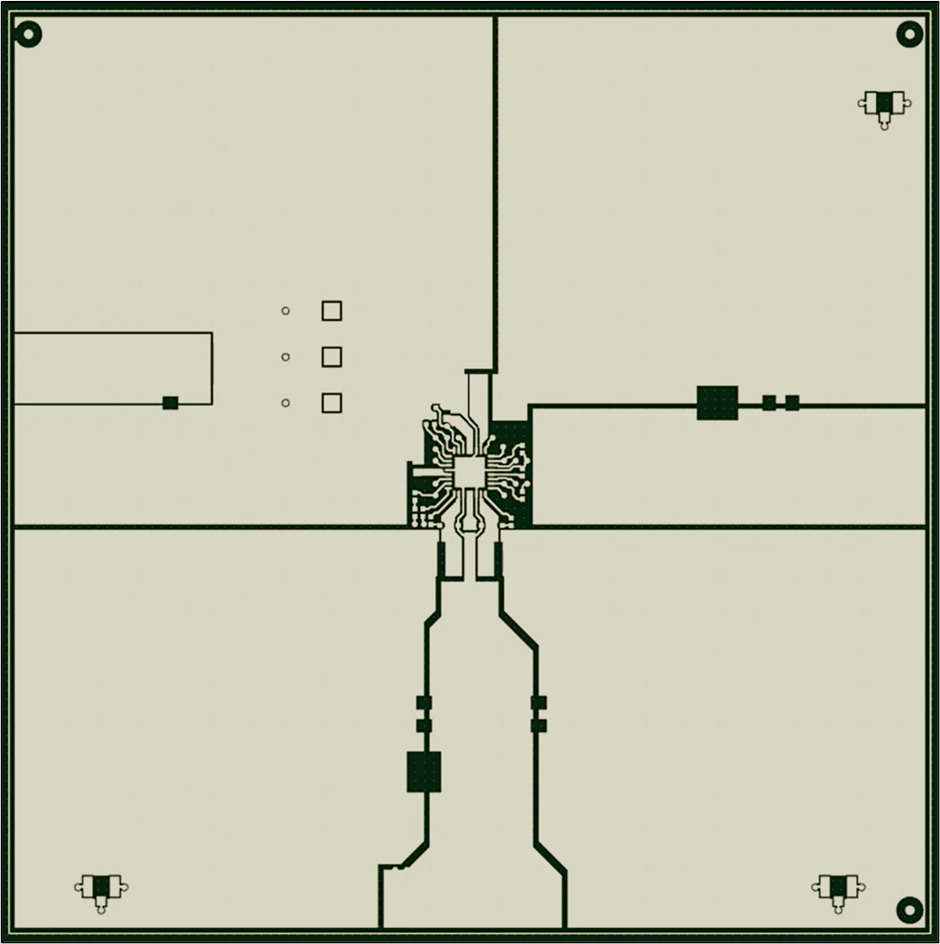
Now, with a single click, move artworks to PCB. This one goes on the top layer. Now these shapes are intelligent design data. You can move or edit them, just like any other data in eCADSTAR, even in 3D.
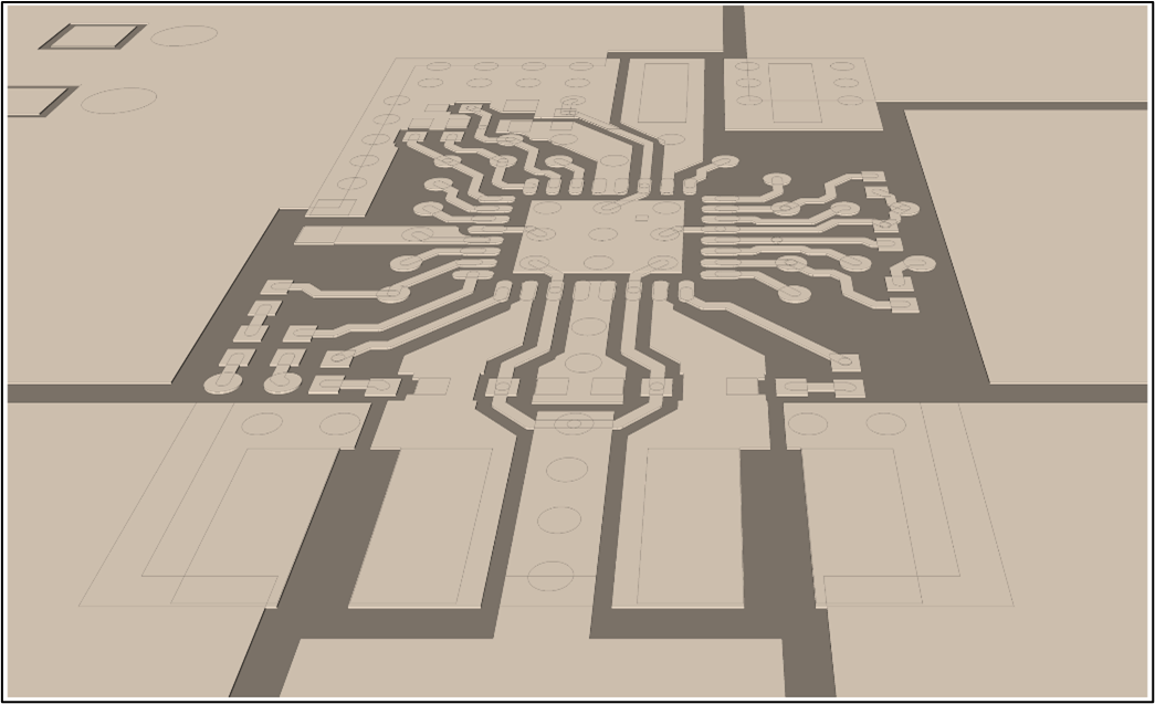
No net information yet, but simply place components that are present in the schematic on transformed artwork and the nets are assigned automatically.
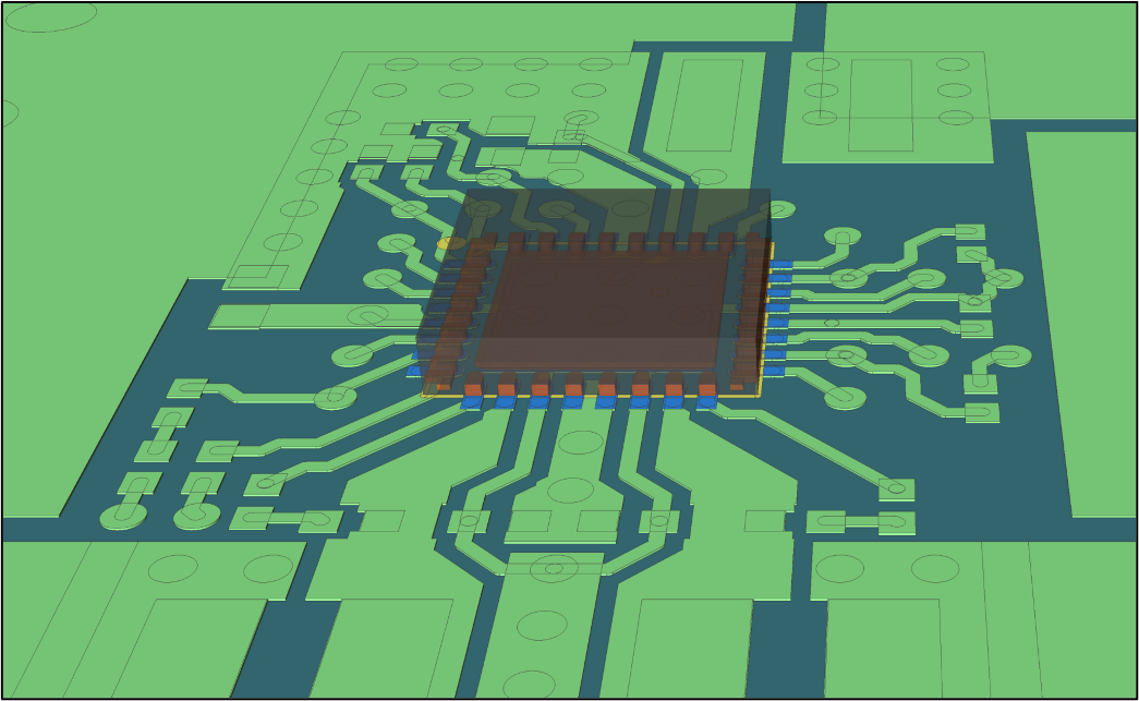
We could equally have done this in reverse, adding the components and nets in PCB Editor and back-annotating them to the schematic. Artworks are physical data and some engineers prefer to work that way, while some want to start with a complete schematic. You can even use just part of an artwork, if, for example, you want to supply input power to the regulator device from a different kind of connector or component. Again, the choice is yours, to give you the most possible re-use opportunities.
Gerber import is incredibly efficient and easy to use. It is one of the most subtle, but also one of the most powerful, capabilities of eCADSTAR for the reuse of designs (even if Gerber data is all you have).
EMBEDDED SI
Signal Integrity is embedded into the eCADSTAR Schematic and PCB Editors providing pre-layout and post-layout simulation capabilities.
- Simulate, measure, share results independently of PCB design.
- Constrain and plan topologies in the pre-layout phase.
- Plan impedance using the integrated field solver using lossy interconnect models.
- Analyze signals in the time domain.
- Automatic measurement for key distortion and timing parameters (e.g. slew rate) allows fast error detection.
WHAT-IF ANALYSIS
Perform what-if analysis to optimize high-speed performance
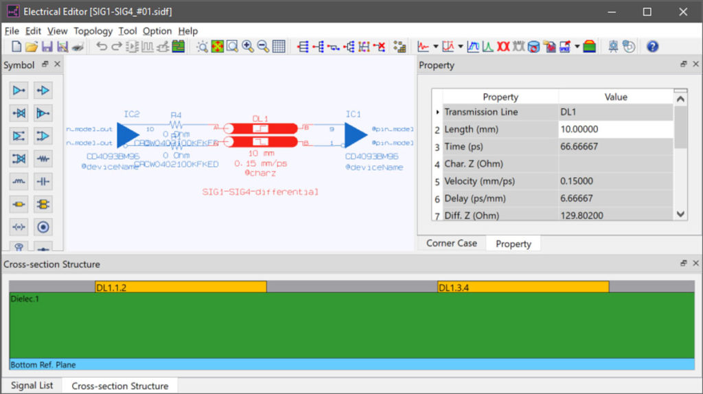
Electrical Editor:
- Extract equivalent electrical topologies based on physical PCB design data (routing and placement).
- Extract coupled/uncoupled transmission line structures with user-defined parameters.
- Detect return path discontinuities by considering true reference plane shapes including routing over cut-outs on reference layers.
- Extract via models (complex vias) and consider back-drilling.
- Consider same-layer reference conductors (Co-planar extraction).
- Perform impedance studies by changing cut-sections in the field solver.
SI ADVANCED
Signal Integrity Advanced for very high-speed design. Builds on the functionality that the Signal Integrity option delivers and adds even more functionality.
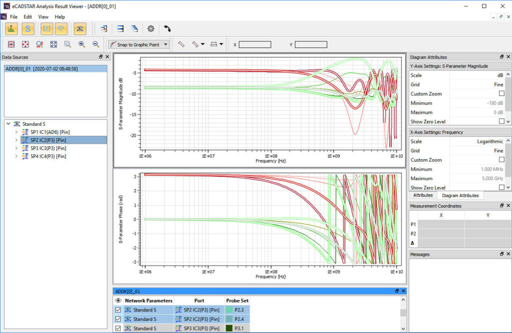
- Derive S-parameters for topologies that you have extracted and edited in Electrical Editor.
- S-Parameters allow modeling passive interconnect behavior in frequency-domain (derived from measurement or like in eCADSTAR by simulation). S-Parameter export from the Electrical editor handles modeling of passive circuit elements only.
- S-Parameters describe coupling and transmission behavior of a system for a wide frequency range. Issues at high frequencies which for example may cause crosstalk can be identified, quickly.
- TDR (Time-Domain-Reflectometry) analysis sends a fast pulse down the PCB trace and displays the returning reflections, which indicate changes in impedance. This allows estimating signal integrity performance without the need to have IBIS buffer models assigned.
ADDRESSING A COMPLEX PROBLEM DOMAIN
To support all relevant high-speed requirements, the key high-speed design issues are:
- Impedance control.
- Skew/length matching & topology control.
- Rule Definition for high-speed routing (e.g. pin-pairs, impedance, max number of vias).
- Designing against these high-speed rules.
- What-if capabilities are needed (e.g. topology, terminations).
- Concurrent SI and PI analysis allows an immediate judgment of the electrical performance for design decisions.
- 6,000+
Delegates trained
- 1,326+
Manufactured Prototype PCBS
- 27,151+
Purchase Orders Raised
- 6,212+
PCB Designs Completed
- 2,221+
PCB Designs Fabricated
- 15,000+
Support Cases Dealt with
eCADSTAR Library Editor
Gold Autodesk Software Reseller for the mechanical and construction industries, sole UK reseller of Zuken’s PCB design software, eCADSTAR and Experienced PCB Design Bureau Specialists. We pride ourselves on our consultative approach to working with customers as their technology partner.


